
Документация
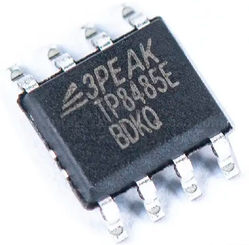
Микросхема TP8485E-SR
У поставщика
У поставщиков
48 416 шт.
Норм. уп.: 25
Цены поставщиков
Склад 39
В наличии:37 114 шт.
Срок поставки: до недели
Норм. уп.: 4000
| Кол-во, шт. | Цена, ₽ |
|---|---|
| от 1 | 12,76 |
| от 315 | 10,98 |
| от 514 | 9,97 |
| от 860 | 9,18 |
| от 1 437 | 8,63 |
Склад 13
В наличии:8 327 шт
Срок поставки: до недели
Норм. уп.: 4000
Минимальная партия: 50 шт
| Кол-во, шт. | Цена, ₽ |
|---|---|
| от 1 | 13,82 |
| от 223 | 12,42 |
| от 446 | 11,29 |
| от 891 | 10,33 |
| от 1 781 | 9,69 |
Склад 15
В наличии:2 975 шт
Срок поставки: до 10 дн.
Норм. уп.: 25
| Кол-во, шт. | Цена, ₽ |
|---|---|
| от 25 | 7,10 |
Описание
Микросхема интерфейса RS-485 от 3PEAK в корпусе SOIC-8 для поверхностного монтажа. Поддерживает скорость передачи от 300 бит/с до 250 кбит/с и работает при напряжении от 3 до 5,5 В. Устройство рассчитано на подключение до 256 узлов на шину и имеет встроенную защиту от электростатических разрядов до ±18 кВ. Подходит для промышленной автоматики и систем сбора данных.
Технические характеристики
| Корпус | SOIC-8 |
| Тип монтажа | SMD |
| Количество | 4000 |
| Скорость передачи данных | 300bps to 250kbps |
| Кол-во выводов | 8 |
| Unit load | 1/8 |
| Описание | ±18K ESD Protection, Full Fail-Safe RS-485 Transceiver |
| Артикул | TP8485E-SR |
| Макс. скорость передачи данных | 250kbps |
| Data rate min | 300bps |
| Number of nodes | 256 |
| Transport media | Tape and Reel |
| Esd hbm bus pins | ±18kV |
| Nodes on bus max | 256 |
| Driver pulse skew | 23ns |
| Макс. вх. ток | 0.012uA |
| Input current min | 0.007uA |
| Тип. входной ток | 0.01uA |
| Esd hbm other pins | ±4kV |
| ESD защита HBM | ±18kV |
| Макс. напр. пит. | 5.5V |
| Мин. напр. пит. | 3V |
| Driver disable time | 250ns |
| Receiver pulse skew | 40ns |
| Bus input current max | 53μA |
| Bus pin voltage range | -15V to +15V |
| Receiver disable time | 7ns |
| Driver enable time max | 562ns |
| Esd protection iec air | ±18kV |
| Driver disable time max | 250ns |
| Макс. темп. хр. | 150°C |
| Мин. темп. хр. | -65°C |
| Driver propagation delay | 340ns |
| Iec fast transient burst | +4kV |
| Макс. темп. перехода | +150°C |
| Receiver enable time max | 989ns |
| Thermal resistance soic8 | 158°C/W |
| Driver rise fall time max | 620ns |
| Макс. раб. темп. | 125°C |
| Мин. раб. темп. | -40°C |
| Receiver disable time max | 7ns |
| Bus input current vcc0 max | -47uA |
| Bus input current vcc0 min | -53uA |
| Bus input current vcc0 typ | -50uA |
| Esd protection iec contact | ±13kV |
| Receiver propagation delay | 960ns |
| Supply current dynamic max | 1.5mA |
| Bus common mode voltage max | +13V |
| Bus common mode voltage min | -8V |
| Receiver hysteresis typical | 110mV |
| Thermal resistance theta ja | 158°C/W |
| Absolute max bus voltage max | 15V |
| Absolute max bus voltage min | -15V |
| Driver output rise fall time | 620ns |
| Driver propagation delay max | 340ns |
| Input voltage range di de re | -0.3V to (VCC + 0.3V) |
| Макс. температура перехода | 150°C |
| Макс. ток покоя | 930μA |
| Receiver output current drive | 25mA |
| Absolute max input voltage max | VCC+0.3V |
| Absolute max input voltage min | -0.3V |
| Bus input current vcc45 55 max | 53uA |
| Bus input current vcc45 55 min | 47uA |
| Bus input current vcc45 55 typ | 50uA |
| Receiver output rise fall time | 12.4ns |
| Receiver propagation delay max | 960ns |
| Absolute max supply voltage max | 7V |
| Absolute max supply voltage min | -0.3V |
| Bus pin transient pulse voltage | ±100V |
| Receiver rise fall time typical | 12.4ns |
| Absolute max bus transient pulse | ±100V |
| Bus pin common mode voltage range | -8V to +13V |
| Esd iec61000 4 2 air gap bus pins | ±18kV |
| Esd iec61000 4 2 contact bus pins | ±13kV |
| Driver enable time receiver enabled | 562ns |
| Receiver enable time driver enabled | 70ns |
| Driver enable time receiver disabled | 562ns |
| Receiver enable time driver disabled | 989ns |
| Driver common mode output voltage max | Vcc/2+0.2V |
| Driver common mode output voltage min | Vcc/2-0.2V |
| Driver common mode output voltage typ | Vcc/2V |
| Esd iec61000 4 4 fast transient burst | +4kV |
| Receiver low level output voltage max | 0.270V |
| Receiver low level output voltage min | 0.240V |
| Receiver low level output voltage typ | 0.240V |
| Receiver negative going threshold max | -145mV |
| Receiver negative going threshold min | -185mV |
| Receiver negative going threshold typ | -160mV |
| Receiver positive going threshold max | -45mV |
| Receiver positive going threshold min | -75mV |
| Receiver positive going threshold typ | -50mV |
| Supply current quiescent disabled max | 1.5uA |
| Supply current quiescent disabled min | 0.7uA |
| Supply current quiescent disabled typ | 1.4uA |
| Driver differential output capacitance | 8pF |
| Receiver high level output voltage max | 4.690V |
| Receiver high level output voltage min | 4.640V |
| Receiver high level output voltage typ | 4.650V |
| Differential output capacitance typical | 8pF |
| Driver short circuit output current max | 115mA |
| Driver short circuit output current min | 75mA |
| Driver short circuit output current typ | 80mA |
| Absolute max receiver output voltage max | VCC+0.3V |
| Absolute max receiver output voltage min | -0.3V |
| Driver differential output voltage min 3v | 1.5V |
| Driver differential output voltage min 5v | 2.5V |
| Receiver differential input hysteresis max | 120mV |
| Receiver differential input hysteresis min | 100mV |
| Receiver differential input hysteresis typ | 110mV |
| Receiver high impedance output current max | 0.011uA |
| Receiver high impedance output current min | -0.005uA |
| Receiver high impedance output current typ | 0.01uA |
| Supply current quiescent driver enabled max | 280uA |
| Supply current quiescent driver enabled min | 210uA |
| Supply current quiescent driver enabled typ | 270uA |
| Driver common mode output voltage change max | 0.2mV |
| Driver common mode output voltage change min | -0.2mV |
| Driver common mode output voltage change typ | 0mV |
| Driver differential output voltage rl60 vcc5 | 2.6V |
| Driver differential output voltage change max | 0.03V |
| Driver differential output voltage change min | -0.02V |
| Driver differential output voltage change typ | -0.002V |
| Supply current quiescent receiver enabled max | 530uA |
| Supply current quiescent receiver enabled min | 440uA |
| Supply current quiescent receiver enabled typ | 480uA |
| Driver differential output voltage rl100 rs422 | 3V |
| Driver peak to peak common mode output voltage | 500mV |
| Driver differential output voltage rl54 vcc3 min | 1.4V |
| Driver differential output voltage rl54 vcc3 typ | 1.5V |
| Driver differential output voltage rl54 vcc5 min | 2.1V |
| Driver differential output voltage rl54 vcc5 typ | 2.5V |
| Receiver differential input threshold negative max | -145mV |
| Receiver differential input threshold negative min | -185mV |
| Receiver differential input threshold positive max | -45mV |
| Receiver differential input threshold positive min | -75mV |
| Supply current quiescent driver receiver enabled max | 930uA |
| Supply current quiescent driver receiver enabled min | 640uA |
| Supply current quiescent driver receiver enabled typ | 695uA |
Заметили ошибку в описании или параметрах?