
Документация
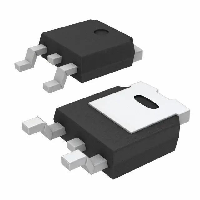
Транзистор полевой MOSFET N-канальный 250В 17A
У поставщика
ПроизводительSTMicroelectronics
КатегорияТранзисторы
У поставщиков
3 585 шт.
Норм. уп.: 5
Цены поставщиков
Склад 13
В наличии:3 505 шт
Срок поставки: до недели
Норм. уп.: 2500
Минимальная партия: 8 шт
| Кол-во, шт. | Цена, ₽ |
|---|---|
| от 1 | 114,39 |
| от 69 | 107,70 |
| от 138 | 103,21 |
| от 275 | 99,27 |
| от 550 | 96,61 |
Склад 12
В наличии:80 шт
Срок поставки: до недели
Норм. уп.: 5
Минимальная партия: 50 шт
| Кол-во, шт. | Цена, ₽ |
|---|---|
| от 1 | 113,85 |
| от 5 | 96,55 |
Описание
Транзистор полевой MOSFET N-канальный от STMicroelectronics. Рабочее напряжение 250 В, ток до 17 А, сопротивление открытого канала 0,14 Ом. Выполнен в компактном корпусе DPAK. Подходит для импульсных источников питания и схем управления нагрузкой в промышленной автоматике.
Технические характеристики
| Тип | N-channel MOSFET |
| Серия | STripFET II |
| Маркировка | 17NF25 |
| Корпус | DPAK |
| Тип монтажа | SMD |
| Без свинца | ECOPACK compliant |
| Упаковка | Tape & reel |
| Описание | N-channel 250V - 0.14 ohm - 17A - DPAK Low gate charge STripFET II Power MOSFET |
| Артикул | STD17NF25 |
| Fall time tf | 8.8ns |
| Rise time tr | 17.2ns |
| Тип. время спада | 8.8ns |
| Тип. время нарастания | 17.2ns |
| Коэф. сниж. | 0.72 W/degC |
| Тип транзистора | N-channel Power MOSFET |
| Gfs test condition | VDS = 15V, ID = 8.5A |
| Vsd test condition | ISD = 17A, VGS = 0 |
| Структура | N-канал |
| Avalanche condition | Tj=25°C, Id=Iar, Vdd=50V |
| Темп. хранения | -55 to 150 degC |
| Current drain pulsed | 68A |
| Rdson test condition | VGS = 10V, ID = 8.5A |
| Total gate charge qg | 29.5nC |
| Avalanche current iar | 17A |
| Gate drain charge qgd | 15.6nC |
| Тип. заряд затвор-сток | 15.6nC |
| Тип. входная емкость | 1000pF |
| Размеры корпуса мм | A: 2.2-2.4; B: 0.64-0.9; C: 0.45-0.6; A1: 0.9-1.1; A2: 0.03-0.23; C2: 0.4 (min); B4: 5.2-5.4 |
| Макс. рассеиваемая мощность | 90W |
| Тип. заряд затвора | 29.5nC |
| Coss eq test condition | VGS = 0, VDS = 0V to 200V |
| Forward on voltage vsd | 1.6V |
| Gate source charge qgs | 4.8nC |
| Тип. заряд затвор-исток | 4.8nC |
| Input capacitance ciss | 1000pF |
| Выходная емкость тип. | 178pF |
| Время задержки вкл. тип. | 8.8ns |
| Avalanche energy single | 100mJ |
| Напряжение затвор-исток макс. | ±20V |
| Gate source voltage vgs | +/-20V |
| Output capacitance coss | 178pF |
| Время задержки выкл. тип. | 21ns |
| Тип упаковки | Tape and Reel (лента в катушке) |
| Current drain continuous | 17A |
| Drain current pulsed idm | 68A |
| Gate input resistance rg | 2 ohm |
| Source drain current isd | 17A |
| Switching test condition | Vdd=125V, Id=8.5A, Rg=4.7Ω, Vgs=10V |
| Turn on delay time td on | 8.8ns |
| Voltage drain source max | 250V |
| Drain source voltage vdss | 250V |
| Forward voltage diode max | 1.6V |
| Пиковое dv/dt восстановления диода | 10 V/ns |
| Диап. темп. хр. | -55 to 150°C |
| Capacitance test condition | VDS = 25V, f = 1MHz, VGS = 0 |
| Gate charge test condition | VDD = 200V, ID = 17A, VGS = 10V |
| Пороговое напряжение затвора макс. | 4V |
| Пороговое напряжение затвора мин. | 2V |
| Тип. пороговое Uзи | 3V |
| Turn off delay time td off | 21ns |
| Forward transconductance gfs | 14S |
| Total power dissipation tc25 | 90W |
| Описание (англ.) | N-channel 250 V, 0.14 Ohm, 17 A |
| Current drain continuous 100c | 10A |
| Drain current continuous tc25 | 17A |
| Gate threshold test condition | VDS = VGS, ID = 250uA |
| Reverse recovery time typ 25c | 157ns |
| Drain current continuous tc100 | 10A |
| Gate body leakage current igss | +/-100nA |
| Max lead soldering temperature | 300 degC |
| Рабочая температура перехода | -55 to 150 degC |
| Resistance drain source on max | 0.165Ω |
| Resistance drain source on typ | 0.14Ω |
| Reverse recovery time trr tc25 | 157ns |
| Reverse recovery time typ 150c | 196ns |
| Forward voltage diode condition | Isd=17A, Vgs=0 |
| Reverse recovery charge typ 25c | 0.91µC |
| Reverse recovery test condition | ISD = 17A, di/dt = 100A/us, VDD = 50V |
| Reverse recovery time trr tc150 | 196ns |
| Gate threshold voltage condition | Vds=Vgs, Id=250µA |
| Reverse recovery charge qrr tc25 | 0.91uC |
| Reverse recovery charge typ 150c | 1.34µC |
| Reverse recovery current typ 25c | 11.6A |
| Обр. проходная емкость тип. | 28pF |
| Source drain current pulsed isdm | 68A |
| Тепловое сопр. переход-корпус | 1.38°C/W |
| Gate threshold voltage vgs th max | 4V |
| Gate threshold voltage vgs th min | 2V |
| Gate threshold voltage vgs th typ | 3V |
| Reverse recovery charge qrr tc150 | 1.34uC |
| Reverse recovery current typ 150c | 13.7A |
| Reverse transfer capacitance crss | 28pF |
| Single pulse avalanche energy eas | 100mJ |
| Макс. темп. перехода | 150°C |
| Мин. темп. перехода | -55°C |
| Reverse recovery current irrm tc25 | 11.6A |
| Reverse recovery current irrm tc150 | 13.7A |
| Тепловое сопротивление переход-среда | 62.5°C/W |
| Resistance drain source on condition | Vgs=10V, Id=8.5A |
| Zero gate voltage drain current idss | 1uA |
| Drain source breakdown test condition | ID = 1mA, VGS = 0 |
| Drain source breakdown voltage vbrdss | 250V |
| Equivalent output capacitance coss eq | 135pF |
| Zero gate voltage drain current idss tc125 | 10uA |
| Static drain source on resistance rdson max | 0.165 ohm |
| Static drain source on resistance rdson typ | 0.14 ohm |
| Максимальное напряжение сток-исток Uси,В | 30 |
| Максимальный ток сток-исток при 25 С Iси макс..А | 20 |
| Обратное напряжение, В | 250 |
| Ток, А | 17 |
Заметили ошибку в описании или параметрах?