
Документация
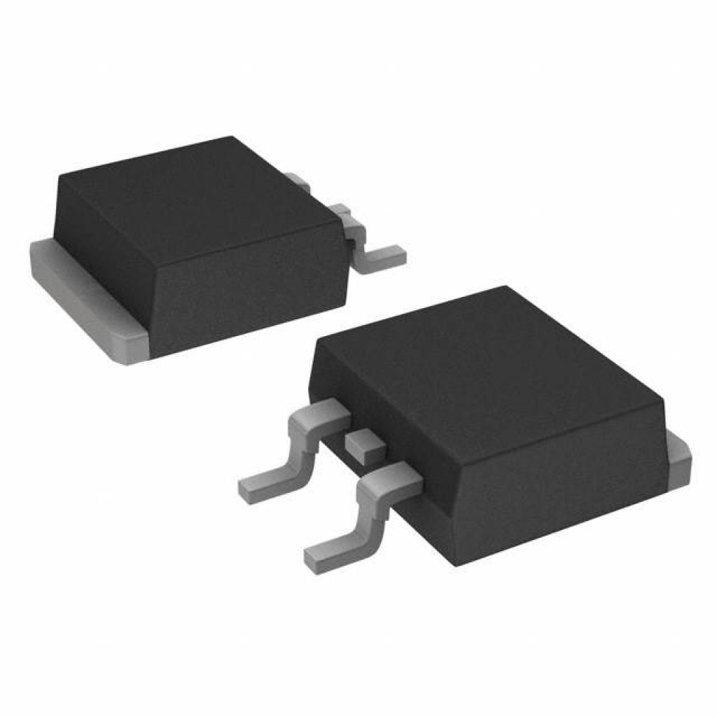
Транзистор полевой MOSFET N-канальный 900В 140Вт
У поставщика
ПроизводительSTMicroelectronics
КатегорияТранзисторы
У поставщиков
7 шт.
Норм. уп.: 1000
Цены поставщиков
Склад 13
В наличии:7 шт
Срок поставки: до недели
Норм. уп.: 1000
Минимальная партия: 8 шт
| Кол-во, шт. | Цена, ₽ |
|---|---|
| от 1 | 101,43 |
| от 14 | 99,71 |
| от 28 | 97,45 |
| от 55 | 94,28 |
| от 109 | 90,24 |
Описание
Транзистор полевой MOSFET N-канальный от STMicroelectronics. Рабочее напряжение 900 В, мощность рассеивания 140 Вт, ток стока 5.8 А. Выполнен в корпусе D2Pak (TO-263) со встроенной Zener-защитой. Применяется в импульсных источниках питания и силовой электронике.
Технические характеристики
| Серия | SuperMESH |
| Маркировка | B6NK90Z |
| Корпус | D2PAK |
| Особенности | Extremely high dv/dt capability, 100% avalanche tested, Gate charge minimized, Very low intrinsic capacitances, Very good manufacturing repeatability, Zener-protected gate |
| Тип монтажа | SMD |
| Упаковка | Tape and reel |
| Код заказа | STB6NK90ZT4 |
| Rds(вкл) макс. | 2 Ohm |
| Rds(вкл) тип. | 1.56 Ohm |
| Применение | Switching application |
| Описание | N-channel 900V - 1.56 Ohm - 5.8A - D2PAK Zener-protected SuperMESH Power MOSFET |
| Артикул | STB6NK90ZT4 |
| Fall time tf | 20ns |
| Rise time tr | 45ns |
| Коэф. сниж. | 1.12 W/°C |
| Тип транзистора | N-channel Power MOSFET |
| Cross over time tc | 20ns |
| Avalanche current iar | 5.8A |
| Gate drain charge qgd | 25nC |
| Gate source charge qgs | 8.5nC |
| Input capacitance ciss | 1350pF |
| Rds on test conditions | VGS=10V, ID=2.9A |
| Coss eq test conditions | VDS=0V to 720V |
| Gate source voltage vgs | ±30V |
| Output capacitance coss | 130pF |
| Тип упаковки | Tape and Reel (лента в катушке) |
| Drain current pulsed idm | 23.2A |
| Total gate charge qg max | 60.5nC |
| Total gate charge qg typ | 46.5nC |
| Turn on delay time td on | 17ns |
| Drain source voltage vdss | 900V |
| Dv dt peak diode recovery | 4.5 V/ns |
| Reverse recovery time trr | 840ns |
| Диап. темп. хр. | -55 to 150 °C |
| Switching test conditions | VDD=450V, ID=3A, RG=4.7 Ohm, VGS=10V |
| Coss eq output capacitance | 70pF |
| Turn off delay time td off | 20ns |
| Условия теста емкости | VDS=25V, f=1MHz, VGS=0 |
| Gate charge test conditions | VDD=720V, ID=5.8A, VGS=10V |
| Reverse recovery charge qrr | 5880uC |
| Diode forward on voltage vsd | 1.6V |
| Forward transconductance gfs | 5S |
| Total power dissipation tc25 | 140W |
| Описание (англ.) | N-channel 900 V, 1.56 Ohm, 5.8 A D2PAK Zener-protected SuperMESH, 140W |
| Diode forward test conditions | ISD=5.8A, VGS=0 |
| Drain current continuous tc25 | 5.8A |
| Off voltage rise time tr voff | 11ns |
| Reverse recovery current irrm | 14A |
| Diode recovery test conditions | ISD=5.8A, di/dt=100A/us, VDD=36V, Tj=150°C |
| Drain current continuous tc100 | 3.65A |
| Gate threshold test conditions | VDS=VGS, ID=100uA |
| Max lead soldering temperature | 300 °C |
| Gate body leakage test conditions | VGS=±20V, VDS=0 |
| Gate source zener test conditions | Igs=±1mA (Open Drain) |
| Gate threshold voltage vgs th max | 4.5V |
| Gate threshold voltage vgs th min | 3V |
| Gate threshold voltage vgs th typ | 3.75V |
| Reverse transfer capacitance crss | 26pF |
| Single pulse avalanche energy eas | 300mJ |
| Gate body leakage current igss max | ±10uA |
| Gate source zener breakdown voltage | 30V |
| Drain source leakage test conditions | VDS=Max Rating, VGS=0 |
| Диапазон темп. перехода | -55 to 150 °C |
| Drain source leakage current idss max | 1uA |
| Thermal resistance junction case rthjc | 0.89 °C/W |
| Thermal resistance junction pcb rthjpcb | 60 °C/W |
| Forward transconductance test conditions | VDS=15V, ID=2.9A |
| Thermal resistance junction ambient rthja | 62.5 °C/W |
| Drain source leakage current idss tc125 max | 50uA |
Заметили ошибку в описании или параметрах?