
Документация
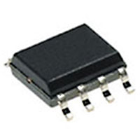
SIT1050T, CAN интерфейс (=TJA1050T) SO8
У поставщика
ПроизводительSIT
У поставщиков
2 шт.
Норм. уп.: 10
Цены поставщиков
Склад 12
В наличии:2 шт
Срок поставки: до недели
Норм. уп.: 10
| Кол-во, шт. | Цена, ₽ |
|---|---|
| от 1 | 38,30 |
| от 10 | 32,26 |
Описание
SIT1050T — это CAN-интерфейс от производителя SIT, совместимый с TJA1050T. Микросхема поддерживает скорость передачи данных до 1 Мбит/с, работает с логикой 3.3В и 5В, доступна в корпусе SOIC-8 для поверхностного или выводного монтажа. Подходит для промышленной автоматики и автомобильных систем связи.
Технические характеристики
| Корпус | SOP8, DIP8 |
| Тип монтажа | SMD (SOP8), THT (DIP8) |
| Корпус | SOIC-8 |
| Совместимость | ISO 11898, 3.3V and 5V logic |
| Макс. скорость передачи данных | 1Mbaud |
| Node count min | 110 |
| Bus voltage range | -40V to +40V |
| Макс. напр. пит. | 5.5V |
| Мин. напр. пит. | 4.5V |
| Txd off current max | 1μA |
| Dominant timeout max | 700μs |
| Dominant timeout min | 300μs |
| Dominant timeout typ | 450μs |
| Driver fall time typ | 50ns |
| Driver rise time typ | 25ns |
| Transient bus voltage | -200V to +200V |
| Power dissipation dip8 | 700mW |
| Power dissipation sop8 | 400mW |
| Receiver fall time typ | 8ns |
| Receiver rise time typ | 8ns |
| Receiver hysteresis min | 100mV |
| Receiver hysteresis typ | 125mV |
| Макс. темп. хр. | 150°C |
| Мин. темп. хр. | -55°C |
| Welding temperature max | 300°C |
| Макс. темп. перехода | 125°C |
| Темп. перехода мин. | -40°C |
| Диапазон синфазного напряжения | -12V to +12V |
| Input resistance matching | -3% to 3% |
| Supply current silent max | 10mA |
| Supply current silent typ | 6mA |
| Enable time from silent max | 1μs |
| Input capacitance canh canl | 13pF |
| Supply current dominant max | 70mA |
| Supply current dominant typ | 50mA |
| Абс. макс. напряжение питания | 6V |
| Supply voltage absolute min | -0.3V |
| Recessive output current max | 2.5mA |
| Recessive output current min | -2.0mA |
| Reference output voltage max | 0.6VCC |
| Reference output voltage min | 0.4VCC |
| Supply current recessive max | 10mA |
| Supply current recessive typ | 6mA |
| Receiver low level output max | 0.4V |
| Receiver low level output typ | 0.2V |
| Common mode output voltage max | 3V |
| Common mode output voltage min | 2V |
| Differential input capacitance | 5pF |
| Input resistance canh canl max | 40kΩ |
| Input resistance canh canl min | 15kΩ |
| Input resistance canh canl typ | 30kΩ |
| Receiver high level output min | 4V |
| Receiver high level output typ | 4.6V |
| Power off bus input current max | 250μA |
| Power off bus input current typ | 165μA |
| Receiver negative threshold max | 650mV |
| Receiver negative threshold typ | 500mV |
| Receiver positive threshold min | 800mV |
| Receiver positive threshold typ | 900mV |
| Txd low level input current max | -10μA |
| Txd low level input current min | -50μA |
| Txd low level input voltage max | 0.8V |
| Txd low level input voltage min | -0.3V |
| Bus recessive output voltage max | 3V |
| Bus recessive output voltage min | 2V |
| Canh dominant output voltage max | 4.5V |
| Canh dominant output voltage min | 2.9V |
| Canl dominant output voltage max | 1.5V |
| Canl dominant output voltage min | 0.8V |
| Txd high level input current max | 2μA |
| Txd high level input current min | -2μA |
| Txd high level input voltage max | VCC+0.3V |
| Txd high level input voltage min | 2V |
| Differential input resistance max | 80kΩ |
| Differential input resistance min | 30kΩ |
| Shutdown junction temperature typ | 160°C |
| Loop delay dominant to recessive max | 190ns |
| Loop delay dominant to recessive min | 90ns |
| Loop delay recessive to dominant max | 190ns |
| Loop delay recessive to dominant min | 90ns |
| Bus dominant differential voltage max | 3V |
| Bus dominant differential voltage min | 1.5V |
| Short circuit output current canh neg | -105mA to -72mA |
| Short circuit output current canh pos | 0.36mA to 1mA |
| Short circuit output current canl neg | -1mA to 0.5mA |
| Short circuit output current canl pos | 71mA to 105mA |
| Bus recessive differential voltage max | 0.05V |
| Bus recessive differential voltage typ | 0.012V |
| Common mode output voltage peak to peak | 30mV |
| Driver propagation delay high to low max | 90ns |
| Driver propagation delay high to low min | 25ns |
| Driver propagation delay high to low typ | 45ns |
| Driver propagation delay low to high max | 120ns |
| Driver propagation delay low to high min | 25ns |
| Driver propagation delay low to high typ | 65ns |
| Receiver propagation delay high to low max | 90ns |
| Receiver propagation delay high to low min | 45ns |
| Receiver propagation delay high to low typ | 70ns |
| Receiver propagation delay low to high max | 130ns |
| Receiver propagation delay low to high min | 60ns |
| Receiver propagation delay low to high typ | 100ns |
Заметили ошибку в описании или параметрах?