
Документация
ИС коррекции коэффициента мощности
У поставщика
ПроизводительSTMicroelectronics
У поставщиков
2 437 шт.
Норм. уп.: 10
Цены поставщиков
Склад 13
В наличии:2 380 шт
Срок поставки: до недели
Норм. уп.: 2500
Минимальная партия: 16 шт
| Кол-во, шт. | Цена, ₽ |
|---|---|
| от 1 | 44,55 |
| от 45 | 40,87 |
| от 89 | 37,86 |
| от 177 | 35,59 |
| от 353 | 33,90 |
Склад 12
В наличии:57 шт
Срок поставки: до недели
Норм. уп.: 10
Минимальная партия: 2 шт
| Кол-во, шт. | Цена, ₽ |
|---|---|
| от 1 | 59,00 |
| от 10 | 53,95 |
Описание
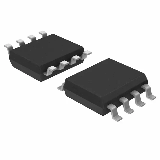
Микросхема коррекции коэффициента мощности от STMicroelectronics. Работает в корпусе SO-8, поставляется на ленте в катушке. Используется в импульсных источниках питания и LED-освещении для повышения энергоэффективности.
Технические характеристики
| Корпус | SO-8 |
| Особенности | Realised in BCD technology, Transition-mode control of PFC pre-regulators, Proprietary multiplier design for minimum THD of AC input current, Very precise adjustable output overvoltage protection, Ultra-low (≤70µA) start-up current, Low (≤4mA) quiescent current, Extended IC supply voltage range, On-chip filter on current sense, Disable function, 1% internal reference voltage, -600/+800mA totem pole gate driver with UVLO pull-down and voltage clamp, DIP-8/SO-8 packages ECOPACK |
| Тип монтажа | SMD |
| Гистерезис | 2.2V to 2.8V |
| Технология | BCD |
| Описание | Transition-mode PFC controller |
| Артикул | L6562DTR |
| Применение | PFC pre-regulators for IEC61000-3-2 compliant SMPS (TV, Desktop PC, Monitor) up to 300W, Hi-end AC-DC adapter/charger, Entry level server & web server |
| Режим управления | Transition Mode (TM) |
| Ovp hysteresis | 30µA |
| Multiplier gain | 0.5 1/V to 0.7 1/V |
| Disable threshold | 150mV to 250mV |
| Restart threshold | 350mV |
| Turn on threshold | 11V to 13V |
| Error amp vref max | 2.535V |
| Error amp vref min | 2.465V |
| Error amp vref typ | 2.5V |
| Turn off threshold | 8.7V to 10.3V |
| Gate driver voh min | 2V |
| Gate driver voh typ | 2.6V |
| Gate driver vol max | 1.9V |
| Gate driver vol min | 0.9V |
| Multiplier gain max | 0.7 1/V |
| Multiplier gain min | 0.5 1/V |
| Multiplier gain typ | 0.6 1/V |
| Startup current max | 70µA |
| Startup current typ | 40µA |
| Uvlo hysteresis min | 2.2V |
| Uvlo hysteresis typ | 2.8V |
| Output clamp voltage | 10V to 15V |
| Start up current max | 70µA |
| Starter timer period | 75µs to 300µs |
| Static ovp threshold | 2.1V to 2.4V |
| Диапазон питания | 10.3V to 22V |
| Vcc on threshold max | 13V |
| Vcc on threshold min | 11V |
| Vcc on threshold typ | 12V |
| Gate driver fall time | 30ns to 70ns |
| Gate driver rise time | 40ns to 80ns |
| Макс. ток покоя | 3.75mA |
| Ток покоя тип. | 2.5mA |
| Vcc off threshold max | 10.3V |
| Vcc off threshold min | 8.7V |
| Vcc off threshold typ | 9.5V |
| Vcc zener voltage max | 28V |
| Vcc zener voltage min | 22V |
| Vcc zener voltage typ | 25V |
| Zener voltage at 20mA | 22V to 28V |
| Error amp sink current | 2.5mA to 4.5mA |
| Произведение усиления на полосу | 1MHz |
| Start timer period max | 300µs |
| Start timer period min | 75µs |
| Start timer period typ | 130µs |
| Thermal resistance so8 | 150°C/W |
| Voltage gain open loop | 60dB to 80dB |
| Zcd arming voltage typ | 2.1V |
| Макс. темп. хр. | 150°C |
| Мин. темп. хр. | -55°C |
| Uvlo saturation voltage | 1.1V max |
| Zcd restart current min | 30µA |
| Zcd restart current typ | 75µA |
| Тип упаковки | Tape and Reel (лента в катушке) |
| Error amp source current | -2mA to -5mA |
| Static ovp threshold max | 2.4V |
| Static ovp threshold min | 2.1V |
| Static ovp threshold typ | 2.25V |
| Zcd max sink current abs | 10mA |
| Gate driver fall time max | 70ns |
| Gate driver fall time typ | 30ns |
| Gate driver rise time max | 80ns |
| Gate driver rise time typ | 40ns |
| Ic supply voltage abs max | self-limited |
| Power dissipation so8 abs | 0.65W |
| Quiescent current ovp typ | 2.2mA |
| Диап. темп. хр. | -55°C to 150°C |
| Zcd disable threshold max | 250mV |
| Zcd disable threshold min | 150mV |
| Zcd disable threshold typ | 200mV |
| Zcd restart threshold typ | 350mV |
| Dynamic ovp hysteresis typ | 30µA |
| Error amp sink current min | 2.5mA |
| Error amp sink current typ | 4.5mA |
| Error amp voltage gain min | 60dB |
| Error amp voltage gain typ | 80dB |
| Power dissipation dip8 abs | 1W |
| Thermal resistance minidip | 100°C/W |
| Zcd input bias current max | 2µA |
| Zcd max source current abs | -50mA |
| Zcd triggering voltage typ | 1.6V |
| Производитель | STM |
| Диап. раб. темп. | -40°C to 150°C |
| Zcd lower clamp voltage max | 1V |
| Zcd lower clamp voltage min | 0.3V |
| Zcd lower clamp voltage typ | 0.65V |
| Zcd upper clamp voltage max | 6.5V |
| Zcd upper clamp voltage min | 5.0V |
| Zcd upper clamp voltage typ | 5.7V |
| Error amp source current max | -5mA |
| Error amp source current min | -2mA |
| Error amp source current typ | -3.5mA |
| Error amp vref over temp max | 2.56V |
| Error amp vref over temp min | 2.44V |
| Operating supply current max | 5mA |
| Operating supply current typ | 3.5mA |
| Supply voltage operating max | 22V |
| Supply voltage operating min | 10.3V |
| Описание (англ.) | Power factor correction IC |
| Analog inputs outputs abs max | -0.3V to 8V |
| Current sense delay to output | 200ns to 350ns |
| Current sense reference clamp | 1.6V to 1.8V |
| Error amp line regulation max | 5mV |
| Error amp line regulation typ | 2mV |
| Error amp lower clamp voltage | 2.1V to 2.4V |
| Error amp upper clamp voltage | 5.3V to 6V |
| Gate driver sink current peak | 800mA |
| Multiplier input bias current | -1µA |
| Restart current after disable | 30µA to 75µA |
| Dynamic ovp triggering current | 35µA to 45µA |
| Current sense clamp voltage max | 1.8V |
| Current sense clamp voltage min | 1.6V |
| Current sense clamp voltage typ | 1.7V |
| Current sense offset at mult 0v | 30mV |
| Current sense offset vmult0 typ | 30mV |
| Gate driver dropout voltage max | 3V |
| Gate driver dropout voltage min | 2.5V |
| Gate driver source current peak | 600mA |
| Gate driver uvlo saturation max | 1.1V |
| Multiplier output max slope min | 1.65V/V |
| Multiplier output max slope typ | 1.9V/V |
| Quiescent current after turn on | 2.5mA to 3.75mA |
| Zcd sink current capability min | 2.5mA |
| Error amp input bias current max | -1µA |
| Current sense delay to output min | 200ns |
| Current sense delay to output typ | 350ns |
| Current sense offset at mult 2.5v | 5mV |
| Current sense offset vmult2 5 typ | 5mV |
| Error amp lower clamp voltage max | 2.4V |
| Error amp lower clamp voltage min | 2.1V |
| Error amp lower clamp voltage typ | 2.25V |
| Error amp upper clamp voltage max | 6V |
| Error amp upper clamp voltage min | 5.3V |
| Error amp upper clamp voltage typ | 5.7V |
| Multiplier input bias current max | -1µA |
| Multiplier linear operation range | 0V to 3V |
| Operating supply current at 70kHz | 3.5mA to 5mA |
| Power dissipation at tamb 50c so8 | 0.65W |
| Reference voltage error amplifier | 2.5V ±1% at 25°C, overall 2.44V to 2.56V |
| Zcd source current capability min | -2.5mA |
| Zcd source current capability typ | -5.5mA |
| Zero current detector lower clamp | 0.3V to 1V |
| Zero current detector upper clamp | 5.0V to 6.5V |
| Dynamic ovp triggering current max | 45µA |
| Dynamic ovp triggering current min | 35µA |
| Dynamic ovp triggering current typ | 40µA |
| Junction temperature operating max | 150°C |
| Junction temperature operating min | -40°C |
| Zero current detector bias current | 2µA |
| Internal reference voltage accuracy | 1% @ Tj=25°C |
| Current sense input bias current max | -1µA |
| Error amp gain bandwidth product typ | 1MHz |
| Gate driver output clamp voltage max | 15V |
| Gate driver output clamp voltage min | 10V |
| Gate driver output clamp voltage typ | 12V |
| Zero current detector arming voltage | 2.1V |
| Current sense comparator bias current | -1µA |
| Multiplier linear operation range max | 3V |
| Multiplier linear operation range min | 0V |
| Gate driver dropout voltage sink 200ma | 0.9V to 1.9V |
| Gate driver dropout voltage source 20ma | 2V to 2.6V |
| Gate driver dropout voltage source 200ma | 2.5V to 3V |
| Zero current detector triggering voltage | 1.6V |
| Thermal resistance junction to ambient so8 | 150 °C/W |
| Zero current detector sink current capability | 2.5mA |
| Zero current detector source current capability | -2.5mA to -5.5mA |
Заметили ошибку в описании или параметрах?