
Документация
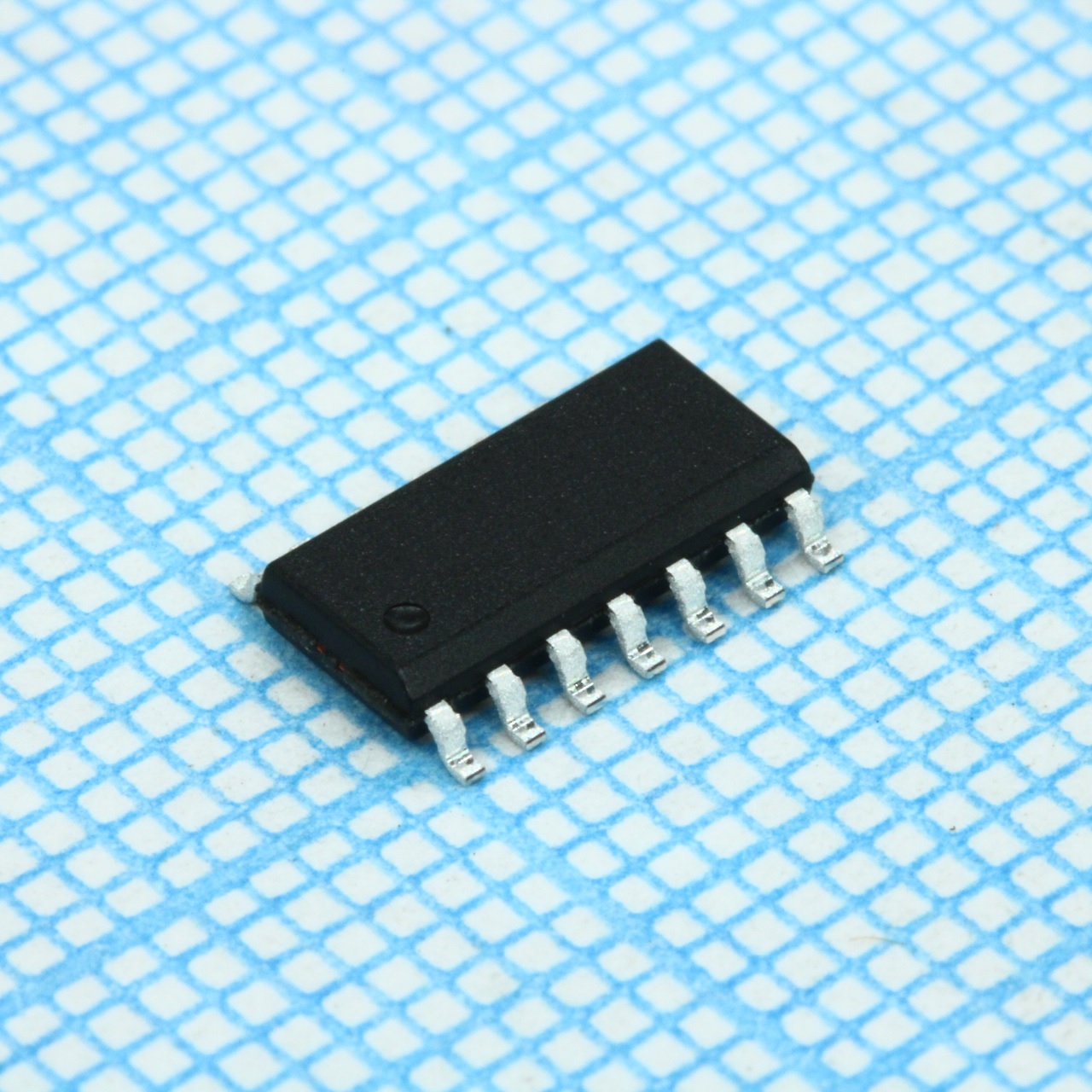
Микросхема IR21844STRPBF
У поставщика
У поставщиков
2 042 шт.
Норм. уп.: 2500
Цены поставщиков
Склад 13
В наличии:2 042 шт
Срок поставки: до недели
Норм. уп.: 2500
Минимальная партия: 6 шт
| Кол-во, шт. | Цена, ₽ |
|---|---|
| от 1 | 155,02 |
| от 48 | 146,61 |
| от 96 | 140,99 |
| от 192 | 136,05 |
| от 384 | 132,70 |
Описание
Микросхема IR21844STRPBF от Infineon представляет собой высоковольтный изолирующий драйвер верхнего и нижнего плеча для мощных IGBT и MOSFET. Устройство обеспечивает надежное управление с защитой от сквозных токов и встроенным опорным напряжением. Применяется в импульсных источниках питания, преобразователях частоты и инверторах для промышленной и бытовой техники.
Технические характеристики
| Корпус | 14-Lead SOIC |
| Тип монтажа | SMD |
| Без свинца | Да |
| Описание | Half-bridge driver, high voltage, high speed power MOSFET and IGBT driver |
| Артикул | IR21844STRPBF |
| Deadtime max rdt 0 | 520ns |
| Deadtime min rdt 0 | 280ns |
| Deadtime typ rdt 0 | 400ns |
| Output sink current | 1.8A |
| Undervoltage lockout | Да |
| Deadtime max rdt 200k | 6µs |
| Deadtime min rdt 200k | 4µs |
| Deadtime typ rdt 200k | 5µs |
| Output source current | 1.4A |
| Turn on rise time max | 60ns |
| Turn on rise time typ | 40ns |
| Turn off fall time max | 35ns |
| Turn off fall time typ | 20ns |
| Макс. темп. окр. среды | 125°C |
| Темп. окружающей среды мин. | -40°C |
| Logic input voltage max | VSS + 10V |
| Logic input voltage min | VSS - 0.3V |
| Макс. темп. хр. | 150°C |
| Мин. темп. хр. | -50°C |
| Тип упаковки | Tape and Reel (лента в катушке) |
| Макс. темп. перехода | 150°C |
| Logic ground voltage max | VCC + 0.3V |
| Logic ground voltage min | VCC - 25V |
| Dead time pin voltage max | VCC + 0.3V |
| Dead time pin voltage min | VSS - 0.3V |
| Input logic compatibility | 3.3V and 5V |
| Logic 0 input voltage max | 0.8V |
| Logic 1 input voltage min | 2.7V |
| Matched propagation delay | Да |
| Power dissipation 14 soic | 1.0W |
| Deadtime matching max rdt 0 | 50ns |
| Gate drive supply range max | 20V |
| Gate drive supply range min | 10V |
| Low side output voltage max | VCC + 0.3V |
| Low side output voltage min | -0.3V |
| Low side supply voltage max | 25V |
| Low side supply voltage min | -0.3V |
| Floating channel max voltage | 600V |
| Low level output voltage max | 0.1V |
| Описание (англ.) | Driver 600V 2.3A 2-OUT High and Low Side Half Brdg Inv/Non-Inv 14-Pin SOIC N T/R |
| High level output voltage max | 1.2V |
| Logic and power ground offset | +/- 5V |
| Turn on propagation delay max | 900ns |
| Turn on propagation delay typ | 680ns |
| Deadtime matching max rdt 200k | 600ns |
| High side floating voltage max | 625V |
| High side floating voltage min | -0.3V |
| Lead temperature soldering 10s | 300°C |
| Logic 0 input bias current max | 1µA |
| Logic 1 input bias current max | 60µA |
| Logic 1 input bias current typ | 25µA |
| Shutdown propagation delay max | 270ns |
| Shutdown propagation delay typ | 180ns |
| Turn off propagation delay max | 400ns |
| Turn off propagation delay typ | 270ns |
| Delay matching hs ls turn on max | 90ns |
| Quiescent vbs supply current max | 150µA |
| Quiescent vbs supply current min | 20µA |
| Quiescent vbs supply current typ | 60µA |
| Quiescent vcc supply current max | 1.6mA |
| Quiescent vcc supply current min | 0.4mA |
| Quiescent vcc supply current typ | 1.0mA |
| Delay matching hs ls turn off max | 40ns |
| Offset supply leakage current max | 50µA |
| Recommended logic input voltage max | VSS + 5V |
| Recommended logic input voltage min | VSS |
| Recommended logic ground voltage max | 5V |
| Recommended logic ground voltage min | -5V |
| High side floating output voltage max | VB + 0.3V |
| High side floating output voltage min | VS - 0.3V |
| Recommended dead time pin voltage max | VCC |
| Recommended dead time pin voltage min | VSS |
| Sd input negative going threshold max | 0.8V |
| Sd input positive going threshold min | 2.7V |
| Рабочая температура | -40°C ~ 125°C |
| Recommended low side output voltage max | VCC |
| Recommended low side output voltage min | 0V |
| Recommended low side supply voltage max | 20V |
| Recommended low side supply voltage min | 10V |
| Allowable offset supply voltage transient | 50V/ns |
| High side floating supply offset voltage max | VB + 0.3V |
| High side floating supply offset voltage min | VB - 25V |
| Thermal resistance junction to ambient 14 soic | 120°C/W |
| Recommended high side floating supply voltage max | VS + 20V |
| Recommended high side floating supply voltage min | VS + 10V |
| Recommended high side floating supply offset voltage max | 600V |
Заметили ошибку в описании или параметрах?