
Документация
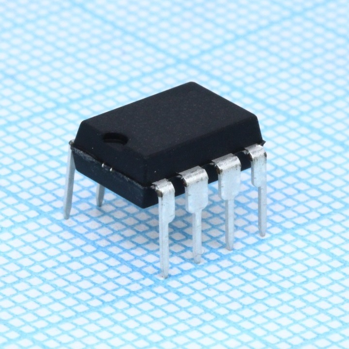
Микросхема IR21531PBF
В наличии
На своём складе
30 шт.
Норм. уп.: 1
У поставщиков
328 шт.
Норм. уп.: 50
Цены (собственный склад)
| Кол-во, шт. | Цена, ₽ |
|---|---|
| от 3 | 110,62 |
| от 6 | 107,65 |
| от 12 | 106,16 |
| от 25 | 103,94 |
Цены поставщиков
Склад 2
В наличии:141 шт
Срок поставки: до 2 недель
| Кол-во, шт. | Цена, ₽ |
|---|---|
| от 3 | 110,62 |
| от 6 | 107,65 |
| от 12 | 106,16 |
| от 25 | 103,94 |
Склад 13
В наличии:187 шт
Срок поставки: до недели
Норм. уп.: 50
| Кол-во, шт. | Цена, ₽ |
|---|---|
| от 1 | 352,53 |
| от 8 | 331,98 |
| от 15 | 315,24 |
| от 29 | 302,78 |
| от 50 | 293,51 |
Описание
Микросхема IR21531PBF от Infineon — это драйвер верхнего и нижнего плеча для MOSFET и IGBT. Работает при напряжении до 600 В, имеет встроенный генератор и защиту от мертвого времени. Подходит для импульсных источников питания, электронных балластов и преобразователей в промышленной и бытовой электронике.
Технические характеристики
| Тип | Драйверы MOSFET и IGBT |
| Корпус | DIP-8 |
| Особенности | Integrated 600V half-bridge gate driver, 15.6V zener clamp on Vcc, True micropower start up, Tighter initial deadtime control, Low temperature coefficient deadtime, Shutdown feature (1/6th Vcc) on CT pin, Increased undervoltage lockout Hysteresis (1V), Lower power level-shifting circuit, Constant LO, HO pulse widths at startup, Lower di/dt gate driver for better noise immunity, Low side output in phase with RT, Internal 50nsec (typ.) bootstrap diode (IR21531D), Excellent latch immunity on all inputs and outputs, ESD protection on all leads, Also available LEAD-FREE |
| Описание | Самоосциллирующий драйвер полумоста |
| Артикул | IR21531PBF |
| Product summary | Tr tf: 80/40ns; V clamp: 15.6V; Рабочий цикл: 50%; Deadtime typ: 0.6µs; V offset max: 600V |
| Предельные значения | Icc supply current max: 25mA; Irt rt pin current max: 5mA; Irt rt pin current min: -5mA; Vct ct pin voltage max: VCC + 0.3V; Vct ct pin voltage min: -0.3V; Vrt rt pin voltage max: VCC + 0.3V; Vrt rt pin voltage min: -0.3V; Ts storage temperature max: 150°C; Ts storage temperature min: -55°C; Tj junction temperature max: 150°C; Tj junction temperature min: -55°C; Vlo low side output voltage max: VCC + 0.3V; Vlo low side output voltage min: -0.3V; Rthja thermal resistance 8 lead dip: 125°C/W; Rthja thermal resistance 8 lead soic: 200°C/W; Pd maximum power dissipation 8 lead dip: 1.0W; Pd maximum power dissipation 8 lead soic: 0.625W; Tl lead temperature soldering 10 seconds: 300°C; Vb high side floating supply voltage max: 625V; Vb high side floating supply voltage min: -0.3V; Vho high side floating output voltage max: VB + 0.3V; Vho high side floating output voltage min: VS - 0.3V; Dvs dt allowable offset voltage slew rate max: 50V/ns; Dvs dt allowable offset voltage slew rate min: -50V/ns; Vs high side floating supply offset voltage max: VB + 0.3V; Vs high side floating supply offset voltage min: VB - 25V |
| Электрические характеристики | Oscillator io characteristics: Ict ct pin current max: 1.0µA; Ict ct pin current typ: 0.001µA; D rt pin duty cycle max: 52%; D rt pin duty cycle min: 48%; D rt pin duty cycle typ: 50%; Fosc oscillator frequency max: 20.6kHz; Fosc oscillator frequency min: 19.4kHz; Fosc oscillator frequency typ: 20kHz; Vrtuv uv mode rt output voltage max: 100mV; Vrtuv uv mode rt output voltage typ: 0V; Fosc oscillator frequency rt 7 43k max: 106kHz; Fosc oscillator frequency rt 7 43k min: 94kHz; Fosc oscillator frequency rt 7 43k typ: 100kHz; Vct lower ct ramp voltage threshold typ: 4.0V; Vct upper ct ramp voltage threshold typ: 8.0V; Vctsd ct voltage shutdown threshold max: 2.4V; Vctsd ct voltage shutdown threshold min: 1.8V; Vctsd ct voltage shutdown threshold typ: 2.1V; Ictuv uv mode ct pin pulldown current max: 1.2mA; Ictuv uv mode ct pin pulldown current min: 0.30mA; Ictuv uv mode ct pin pulldown current typ: 0.70mA; Vrt low level rt output voltage irt 1ma max: 300mV; Vrt low level rt output voltage irt 1ma typ: 100mV; Vrtsd sd mode rt output voltage irt 1ma max: 300mV; Vrtsd sd mode rt output voltage irt 1ma typ: 10mV; Vrt high level rt output voltage irt 1ma max: 300mV; Vrt high level rt output voltage irt 1ma typ: 100mV; Vrt low level rt output voltage irt 100ua max: 50mV; Vrt low level rt output voltage irt 100ua typ: 10mV; Vrtsd sd mode rt output voltage irt 100ua max: 50mV; Vrtsd sd mode rt output voltage irt 100ua typ: 10mV; Vrt high level rt output voltage irt 100ua max: 50mV; Vrt high level rt output voltage irt 100ua typ: 10mV; Floating supply characteristics: Ilk offset supply leakage current max: 50µA; Iqbs quiescent vbs supply current max: 50µA; Iqbs quiescent vbs supply current typ: 30µA; Vf bootstrap diode forward voltage max: 1.0V; Vf bootstrap diode forward voltage min: 0.5V; Vbsmin minimum required vbs voltage max: 5.0V; Vbsmin minimum required vbs voltage typ: 4.0V; Iqbsuv micropower startup vbs supply current max: 10µA; Iqbsuv micropower startup vbs supply current typ: 0µA; Gate driver output characteristics: Td output deadtime max: 0.85µs; Td output deadtime min: 0.35µs; Td output deadtime typ: 0.60µs; Tf output fall time max: 100ns; Tf output fall time typ: 45ns; Tr output rise time max: 150ns; Tr output rise time typ: 80ns; Vol low level output voltage max: 100mV; Vol low level output voltage typ: 0mV; Voh high level output voltage max: 100mV; Voh high level output voltage typ: 0mV; Vol uv uv mode output voltage max: 100mV; Vol uv uv mode output voltage typ: 0mV; Tsd shutdown propogation delay typ: 660ns; Low voltage supply characteristics: Vclamp vcc zener clamp voltage max: 16.8V; Vclamp vcc zener clamp voltage min: 14.4V; Vclamp vcc zener clamp voltage typ: 15.6V; Iqcc quiescent vcc supply current max: 950µA; Iqcc quiescent vcc supply current typ: 500µA; Vccuvh vcc undervoltage lockout hysteresis max: 1.5V; Vccuvh vcc undervoltage lockout hysteresis min: 0.5V; Vccuvh vcc undervoltage lockout hysteresis typ: 1.0V; Iqccuv micropower startup vcc supply current max: 150µA; Iqccuv micropower startup vcc supply current typ: 75µA; Vccuv rising vcc undervoltage lockout threshold max: 9.9V; Vccuv rising vcc undervoltage lockout threshold min: 8.1V; Vccuv rising vcc undervoltage lockout threshold typ: 9.0V; Vccuv falling vcc undervoltage lockout threshold max: 8.8V; Vccuv falling vcc undervoltage lockout threshold min: 7.2V; Vccuv falling vcc undervoltage lockout threshold typ: 8.0V |
| Recommended component values | Rt timing resistor value min: 10kΩ; Ct ct pin capacitor value min: 330pF |
| Recommended operating conditions | Icc supply current max: 5mA; Vcc supply voltage max: VCLAMP; Vcc supply voltage min: 10V; Tj junction temperature max: 125°C; Tj junction temperature min: -40°C; Vbs high side floating supply voltage max: VCLAMP; Vbs high side floating supply voltage min: VCC - 0.7V; Vs steady state high side floating supply offset voltage max: 600V; Vs steady state high side floating supply offset voltage min: -3.0V |
| Тип монтажа | Выводной |
Заметили ошибку в описании или параметрах?