
Документация
Драйвер полумостовой, Uсм=200В, Uвых=-9.8/15В, Iвых =0.35/0.65А
У поставщика
ПроизводительON Semiconductor
КатегорияМикросхемы
У поставщиков
1 890 шт.
Норм. уп.: 3000
Цены поставщиков
Склад 13
В наличии:1 890 шт
Срок поставки: до недели
Норм. уп.: 3000
Минимальная партия: 10 шт
| Кол-во, шт. | Цена, ₽ |
|---|---|
| от 1 | 83,20 |
| от 51 | 77,53 |
| от 101 | 73,03 |
| от 202 | 69,08 |
| от 403 | 66,42 |
Описание
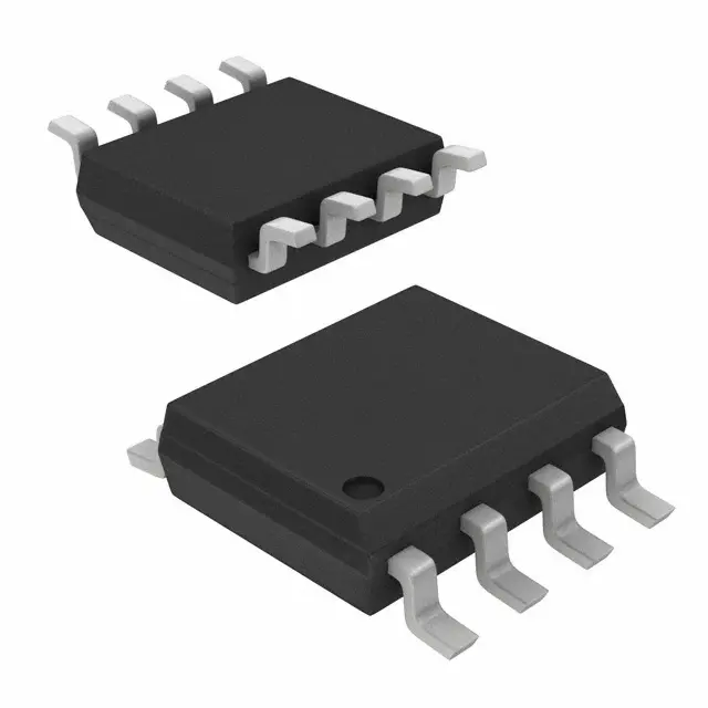
Драйвер полумостовой от ON Semiconductor. Работает при напряжении до 200 В, выходной ток до 0,65 А, напряжение управления до 15 В. Выпускается в компактном корпусе SO-8. Подходит для импульсных источников питания и преобразователей напряжения в промышленной автоматике.
Технические характеристики
| Корпус | 8-SOP |
| Без свинца | Да |
| Тип монтажа | SMD |
| Описание | High and Low Side Gate Driver |
| Артикул | FAN7842MX |
| Метод упаковки | Tape & Reel |
| Logic ground max | VCC +0.3V |
| Logic ground min | VCC -25V |
| Рассеиваемая мощность | 0.625W |
| Темп. хранения | 150°C |
| Vcc uvlo hysteresis | 0.6V |
| Delay matching hs ls | 50ns |
| Темп. перехода | 150°C |
| Рабочий диапазон температур | -40°C to +125°C |
| Макс. рабочее напряжение | 200V |
| Turn on rise time max | 140ns |
| Turn on rise time min | 20ns |
| Turn on rise time typ | 60ns |
| Turn off fall time min | 30ns |
| Turn off fall time typ | 80ns |
| Logic input voltage max | VCC +0.3V |
| Logic input voltage min | -0.3V |
| Output current sink typ | 650mA |
| Тип упаковки | Tape and Reel (лента в катушке) |
| Supply voltage range max | 20V |
| Supply voltage range min | 10V |
| Logic 0 input voltage max | 0.8V |
| Logic 1 input voltage min | 2.9V |
| Output current source typ | 350mA |
| Low side output voltage max | VCC +0.3V |
| Low side output voltage min | -0.3V |
| Low side supply voltage max | 25V |
| Low side supply voltage min | -0.3V |
| High side offset voltage max | +0.3V |
| High side offset voltage min | -25V |
| Low level output voltage max | 0.6V |
| Описание (англ.) | Driver 200V 0.65A 2-OUT Hi/Lo Side Full Brdg/Half Brdg Non-Inv 8-Pin SOP T/R |
| High level output voltage max | 1.0V |
| Turn on propagation delay max | 300ns |
| Turn on propagation delay min | 100ns |
| Turn on propagation delay typ | 170ns |
| Logic 0 input bias current max | 2.0µA |
| Logic 0 input bias current min | 1.0µA |
| Logic 1 input bias current max | 20µA |
| Logic 1 input bias current min | 10µA |
| Turn off propagation delay max | 300ns |
| Turn off propagation delay min | 100ns |
| Turn off propagation delay typ | 200ns |
| Operating vbs supply current typ | 600µA |
| Operating vcc supply current typ | 600µA |
| Quiescent vbs supply current max | 120µA |
| Quiescent vbs supply current typ | 45µA |
| Quiescent vcc supply current max | 180µA |
| Quiescent vcc supply current typ | 70µA |
| Offset supply leakage current max | 10µA |
| Allowable offset voltage slew rate | 50V/ns |
| Recommended ambient temperature max | 125°C |
| Recommended ambient temperature min | -40°C |
| Allowable negative vs pin voltage max | -7.0V |
| Allowable negative vs pin voltage min | -9.8V |
| High side floating output voltage max | VB +0.3V |
| High side floating output voltage min | VS -0.3V |
| High side floating supply voltage max | 225V |
| High side floating supply voltage min | -0.3V |
| Vcc uvlo negative going threshold max | 9.6V |
| Vcc uvlo negative going threshold min | 7.6V |
| Vcc uvlo negative going threshold typ | 8.7V |
| Vcc uvlo positive going threshold max | 10.0V |
| Vcc uvlo positive going threshold min | 8.2V |
| Vcc uvlo positive going threshold typ | 9.2V |
| Термосопротивление переход-среда | 200°C/W |
| Recommended low side supply voltage max | 20V |
| Recommended low side supply voltage min | 10V |
| Output low short circuit pulse current min | 500mA |
| Output low short circuit pulse current typ | 650mA |
| Output high short circuit pulse current min | 250mA |
| Output high short circuit pulse current typ | 350mA |
| Recommended high side floating supply voltage max | VS +20V |
| Recommended high side floating supply voltage min | VS +10V |
| Recommended high side floating supply offset voltage max | 200V |
| Recommended high side floating supply offset voltage min | 6-VCC |
Заметили ошибку в описании или параметрах?