
Документация
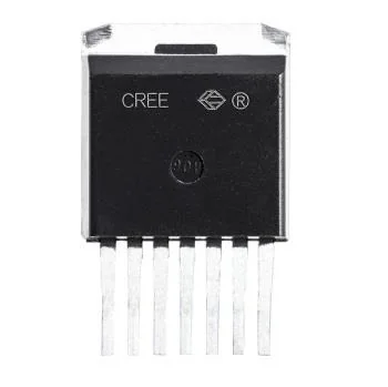
Транзистор полевой MOSFET N-канальный SiC 1200В 7.2А TO-263-7
У поставщика
ПроизводительWolfspeed
КатегорияТранзисторы
У поставщиков
28 шт.
Норм. уп.: 50
Цены поставщиков
Склад 13
В наличии:28 шт
Срок поставки: до недели
Норм. уп.: 50
| Кол-во, шт. | Цена, ₽ |
|---|---|
| от 1 | 725,33 |
| от 4 | 687,27 |
| от 8 | 656,28 |
| от 15 | 633,27 |
| от 29 | 616,15 |
Описание
Транзистор полевой MOSFET N-канальный SiC от Wolfspeed. Рассчитан на напряжение 1200 В и ток 7,2 А, выпускается в корпусе TO-263-7. Применяется в силовой электронике, импульсных источниках питания и промышленной автоматике.
Технические характеристики
| Корпус | TO-263-7 |
| Тип монтажа | SMD |
| Время спада | 11ns |
| Кол-во выводов | 7 |
| Время нарастания | 7ns |
| Технология | Silicon Carbide (SiC) MOSFET |
| Артикул | C3M0350120J |
| Channel type | N-Channel Enhancement Mode |
| Производитель | Wolfspeed |
| Driver source pin | Да |
| Вх. емкость | 345pF |
| Рассеиваемая мощность | 40.8W |
| Полный заряд затвора | 13nC |
| Выходная емкость | 20pF |
| Температура пайки | 260°C |
| Время задержки включения | 6ns |
| Diode pulse current | 20A |
| Темп. хранения | -55 to +150°C |
| Время задержки выключения | 9ns |
| Напряжение сток-исток | 1200V |
| Fall time conditions | VDD = 800V, VGS = -4V/15V, ID = 3.6A, RG(ext) = 0Ω, inductive load |
| Gate to drain charge | 4.6nC |
| Импульсный ток стока | 20A |
| Rise time conditions | VDD = 800V, VGS = -4V/15V, ID = 3.6A, RG(ext) = 0Ω, inductive load |
| Transconductance typ | 2.9S |
| Gate to source charge | 5.1nC |
| Время обратного восстановления | 5ns |
| Напряжение затвор-исток макс. | +19V / -8V |
| Заряд обратного восстановления | 23nC |
| Тип упаковки | Tube (туба) |
| Continuous drain current | 7.2A |
| Internal gate resistance | 7Ω |
| Turn on switching energy | 46µJ |
| Тип. прямое напряжение диода | 4.5V |
| Transconductance 150c typ | 2.6S |
| Turn off switching energy | 8µJ |
| Пороговое напряжение затвора макс. | 3.6V |
| Пороговое напряжение затвора мин. | 1.8V |
| Тип. пороговое Uзи | 2.5V |
| Transconductance conditions | VDS = 20V, ID = 3.6A |
| Input capacitance conditions | VGS = 0V, VDS = 1000V, f = 1MHz |
| Power dissipation conditions | TC = 25°C, TJ = 150°C |
| Обратная проходная емкость | 3.4pF |
| Total gate charge conditions | VDS = 800V, VGS = -4V/15V, ID = 3.6A |
| Описание (англ.) | 1200 V, 7.2 A 3rd‑generation SiC N‑channel MOSFET in a TO‑263‑7 |
| Непрерывный ток стока 100°C | 5A |
| Output capacitance conditions | VGS = 0V, VDS = 1000V, f = 1MHz |
| Peak reverse recovery current | 8A |
| Solder temperature conditions | According to JEDEC J-STD-020 |
| Turn on delay time conditions | VDD = 800V, VGS = -4V/15V, ID = 3.6A, RG(ext) = 0Ω, inductive load |
| Creepage distance drain source | 7mm |
| Diode forward voltage 150c typ | 4.0V |
| Diode pulse current conditions | VGS = -4V, pulse width limited by TJ max |
| Макс. Rси вкл. | 455mΩ |
| Drain source on resistance typ | 350mΩ |
| Рабочая температура перехода | -55 to +150°C |
| Turn off delay time conditions | VDD = 800V, VGS = -4V/15V, ID = 3.6A, RG(ext) = 0Ω, inductive load |
| Drain source voltage conditions | TC = 25°C |
| Gate source leakage current max | 250nA |
| Gate source leakage current typ | 10nA |
| Gate source voltage operational | -4V / 15V |
| Gate threshold voltage 150c typ | 2.0V |
| Gate to drain charge conditions | VDS = 800V, VGS = -4V/15V, ID = 3.6A |
| Pulsed drain current conditions | VGS = 15V, TC = 25°C |
| Continuous diode forward current | 7.3A |
| Diode forward voltage conditions | VGS = -4V, ISD = 1.8A |
| Gate to source charge conditions | VDS = 800V, VGS = -4V/15V, ID = 3.6A |
| Output capacitance stored energy | 10.6µJ |
| Reverse recovery time conditions | VGS = -4V, ISD = 3.6A, VDS = 800V, dI/dt = 3550A/µs, TJ = 150°C |
| Transconductance 150c conditions | VDS = 20V, ID = 3.6A, TJ = 150°C |
| Gate threshold voltage conditions | VDS = VGS, ID = 1mA |
| Gate source voltage max conditions | Transient |
| Reverse recovery charge conditions | VGS = -4V, ISD = 3.6A, VDS = 800V, dI/dt = 3550A/µs, TJ = 150°C |
| Continuous drain current conditions | VGS = 15V, TC = 25°C, TJ ≤ 150°C |
| Drain source on resistance 150c typ | 525mΩ |
| Internal gate resistance conditions | f = 1MHz, VAC = 25mV |
| Тепл. сопр. переход-корпус | 2.9°C/W |
| Turn on switching energy conditions | VDS = 800V, VGS = -4V/15V, ID = 3.6A, RG(ext) = 2.5Ω, L = 716µH |
| Zero gate voltage drain current max | 50µA |
| Zero gate voltage drain current typ | 1µA |
| Turn off switching energy conditions | VDS = 800V, VGS = -4V/15V, ID = 3.6A, RG(ext) = 2.5Ω, L = 716µH |
| Diode forward voltage 150c conditions | VGS = -4V, ISD = 1.8A, TJ = 150°C |
| Drain source on resistance conditions | VGS = 15V, ID = 3.6A |
| Gate source leakage current conditions | VGS = 15V, VDS = 0V |
| Gate threshold voltage 150c conditions | VDS = VGS, ID = 1mA, TJ = 150°C |
| Reverse transfer capacitance conditions | VGS = 0V, VDS = 1000V, f = 1MHz |
| Continuous drain current 100c conditions | VGS = 15V, TC = 100°C, TJ ≤ 150°C |
| Peak reverse recovery current conditions | VGS = -4V, ISD = 3.6A, VDS = 800V, dI/dt = 3550A/µs, TJ = 150°C |
| Drain source on resistance 150c conditions | VGS = 15V, ID = 3.6A, TJ = 150°C |
| Gate source voltage operational conditions | Static |
| Zero gate voltage drain current conditions | VDS = 1200V, VGS = 0V |
| Continuous diode forward current conditions | VGS = -4V |
Заметили ошибку в описании или параметрах?