
Документация
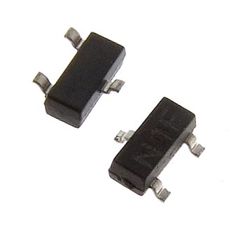
Транзистор BSS84PH6327XTSA2
У поставщика
У поставщиков
45 972 шт.
Норм. уп.: 3000
Цены поставщиков
Склад 13
В наличии:45 972 шт
Срок поставки: до недели
Норм. уп.: 3000
Минимальная партия: 158 шт
| Кол-во, шт. | Цена, ₽ |
|---|---|
| от 1 | 4,38 |
| от 81 | 3,92 |
| от 134 | 3,52 |
| от 267 | 3,23 |
| от 533 | 3,00 |
Описание
Транзистор BSS84PH6327XTSA2 от Infineon — это P-канальный полевой МОП-транзистор с изолированным затвором. Компонент предназначен для коммутации нагрузок и управления питанием в компактных электронных схемах. Отличается низким сопротивлением открытого канала и оптимизирован для поверхностного монтажа.
Технические характеристики
| Mode | Enhancement mode |
| Grade | Automotive |
| Цоколевка | Pin1: Gate; Pin2: Source; Pin3: Drain |
| Серия | SIPMOS Small-Signal-Transistor |
| Маркировка | YBs |
| Корпус | PG-SOT-23 |
| FET Type | P-Channel |
| Тип монтажа | SMD |
| Vgs (Max) | ±20V |
| Esd class | Class 0 (JESD22-A114-HBM) |
| Technology | MOSFET (Metal Oxide) |
| Описание | P-Channel Enhancement Mode MOSFET |
| Dv dt rated | Да |
| Logic level | Да |
| Артикул | BSS84PH6327XTSA2 |
| Channel type | P-Channel |
| Без галогенов | Да |
| Mounting Type | Surface Mount |
| Qualification | AEC-Q101 |
| Reverse diode | Reverse recovery time trr max: 34ns; Reverse recovery time trr typ: 23ns; Reverse recovery charge qrr max: 15nC; Reverse recovery charge qrr typ: 10nC; Inverse diode forward voltage vsd max: -1.24V; Inverse diode forward voltage vsd typ: -0.93V; Inverse diode direct current pulsed ism: -0.68A; Inverse diode continuous forward current is ta25: -0.17A |
| Лента и катушка | H6327: 3000pcs/reel; H6433: 10000pcs/reel |
| Package / Case | TO-236-3, SC-59, SOT-23-3 |
| Avalanche rated | Да |
| Описание | MOSFET P-CH 60V 170MA SOT23-3 |
| Климатическая категория | 55/150/56 (DIN IEC 68-1) |
| Vgs(th) (Max) @ Id | 2V @ 20µA |
| AEC-Q101 | Да |
| Структура | P-канал |
| Operating Temperature | -55°C ~ 150°C (TJ) |
| Rds On (Max) @ Id, Vgs | 8Ohm @ 170mA, 10V |
| Static characteristics | Gate threshold voltage vgsth max: -2V; Gate threshold voltage vgsth min: -1V; Gate threshold voltage vgsth typ: -1.5V; Gate source leakage current igss max: -100nA; Gate source leakage current igss typ: -10nA; Drain source breakdown voltage vbrdss: -60V; Drain source on resistance rds on vgs10 max: 8Ω; Drain source on resistance rds on vgs10 typ: 5.8Ω; Drain source on resistance rds on vgs4 5 max: 12Ω; Drain source on resistance rds on vgs4 5 typ: 8Ω; Zero gate voltage drain current idss ta25 max: -1µA; Zero gate voltage drain current idss ta25 typ: -0.1µA; Zero gate voltage drain current idss ta125 max: -100µA; Zero gate voltage drain current idss ta125 typ: -10µA |
| Power Dissipation (Max) | 360mW (Ta) |
| Supplier Device Package | PG-SOT23 |
| Dynamic characteristics | Fall time tf max: 30.8ns; Fall time tf typ: 20.5ns; Rise time tr max: 24.3ns; Rise time tr typ: 16.2ns; Transconductance gfs min: 0.065S; Transconductance gfs typ: 0.13S; Input capacitance ciss max: 19pF; Input capacitance ciss typ: 15pF; Output capacitance coss max: 8pF; Output capacitance coss typ: 6pF; Turn on delay time td on max: 10ns; Turn on delay time td on typ: 6.7ns; Turn off delay time td off max: 12.9ns; Turn off delay time td off typ: 8.6ns; Reverse transfer capacitance crss max: 3pF; Reverse transfer capacitance crss typ: 2pF |
| Тепл. хар-ки | Тепловое сопротивление переход-точка пайки: 200K/W; Thermal resistance junction ambient rthja 6cm2 cooling: 300K/W; Thermal resistance junction ambient rthja min footprint: 350K/W |
| Предельные значения | Reverse diode dv dt: -6kV/µs; Gate source voltage vgs: ±20V; Drain source voltage vds: -60V; Storage temperature tstg: -55... +150°C; Power dissipation ptot ta25: 0.36W; Pulsed drain current id puls: -0.68A; Avalanche energy periodic ear: 0.036mJ; Continuous drain current id ta25: -0.17A; Continuous drain current id ta70: -0.14A; Avalanche energy single pulse eas: 2.6mJ; Operating junction temperature tj: -55... +150°C |
| Gate charge characteristics | Gate charge total qg max: 1.5nC; Gate charge total qg typ: 1nC; Gate to drain charge qgd max: 0.45nC; Gate to drain charge qgd typ: 0.3nC; Gate to source charge qgs max: 0.37nC; Gate to source charge qgs typ: 0.25nC; Gate plateau voltage vplateau typ: -3.42V |
| Gate Charge (Qg) (Max) @ Vgs | 1.5 nC @ 10 V |
| Drain to Source Voltage (Vdss) | 60 V |
| Input Capacitance (Ciss) (Max) @ Vds | 19 pF @ 25 V |
| Drive Voltage (Max Rds On, Min Rds On) | 4.5V, 10V |
| Current - Continuous Drain (Id) @ 25°C | 170mA (Ta) |
| Тип | MOSFET |
Заметили ошибку в описании или параметрах?