
Документация
Сборка из полевых транзисторов, N+P-канальный, 30 В, 7.2 А/5.3 А, 2 Вт
У поставщика
ПроизводительA&O
КатегорияТранзисторы полевые (FETs, MOSFETs)
У поставщиков
163 шт.
Норм. уп.: 100
Цены поставщиков
Склад 13
В наличии:163 шт
Срок поставки: до недели
Норм. уп.: 100
Минимальная партия: 34 шт
| Кол-во, шт. | Цена, ₽ |
|---|---|
| от 1 | 20,38 |
| от 37 | 18,73 |
| от 74 | 17,20 |
| от 200 | 16,05 |
| от 300 | 15,02 |
Описание
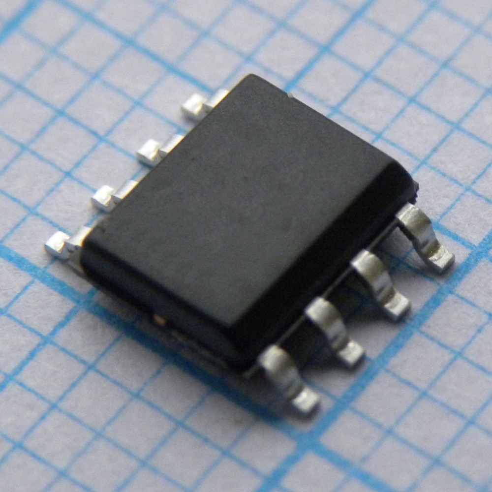
Сборка из полевых транзисторов от A&O, N+P-канального типа. Рабочее напряжение 30 В, токи до 7.2 А и 5.3 А, мощность рассеивания 2 Вт. Компонент выполнен в компактном корпусе SO-8. Подходит для схем управления питанием и защиты в промышленной автоматике.
Технические характеристики
| Тип | MOSFET (N+P-channel complementary) |
| Корпус | SOIC-8 |
| Тип монтажа | SMD |
| Описание | Complementary Enhancement Mode Field Effect Transistor, N+P-channel |
| Название компонента | AO4620 |
| Особенности | 100% UIS tested, 100% Rg tested |
| Gate leakage current | ±100nA |
| Напряжение затвор-исток макс. | ±20V |
| Тип упаковки | Tape and Reel (лента в катушке) |
| Gate resistance n channel | 2.8Ω max |
| Диап. темп. хр. | -55°C to 150°C |
| Switching times n channel | td_on 4.5ns, tr 2.7ns, td_off 14.9ns, tf 2.9ns |
| Avalanche energy n channel | 12mJ (typ), 43mJ (max) |
| Avalanche energy p channel | 43mJ (typ) |
| Диапазон темп. перехода | -55°C to 150°C |
| Avalanche current n channel | 9A |
| Avalanche current p channel | 17A |
| Input capacitance n channel | 448pF max |
| Input capacitance p channel | 760pF (typ) |
| Power dissipation n channel | 2W (T_A=25°C), 1.44W (T_A=70°C) |
| Power dissipation p channel | 2W (T_A=25°C), 1.44W (T_A=70°C) |
| Output capacitance n channel | 67pF (typ) |
| Описание (англ.) | field-effect transistor assembly, N+P-channel, 30V 7.2A/5.3A 2W |
| Pulsed drain current n channel | 64A |
| Pulsed drain current p channel | -40A |
| Voltage drain source n channel | 30V |
| Voltage drain source p channel | -30V |
| Diode forward voltage n channel | 0.74V typ, 1V max |
| Diode forward voltage p channel | -0.8V typ, -1V max |
| Gate charge total 10v n channel | 11nC max |
| Gate charge total 4 5v n channel | 3.5nC (typ) |
| Gate threshold voltage n channel | 1.5V to 2.6V |
| Gate threshold voltage p channel | -1.3V to -2.4V |
| Continuous drain current n channel | 7.2A |
| Continuous drain current p channel | -5.3A |
| Forward transconductance n channel | 20S |
| Forward transconductance p channel | 19S |
| Reverse transfer capacitance n channel | 41pF (typ) |
| Drain source breakdown voltage n channel | 30V min |
| Drain source breakdown voltage p channel | -30V min |
| Drain source on resistance n channel 10v | 24mΩ max (V_GS=10V, I_D=7.2A) |
| Drain source on resistance p channel 10v | 32mΩ max (V_GS=-10V, I_D=-5.3A) |
| Drain source on resistance n channel 4 5v | 36mΩ max (V_GS=4.5V, I_D=5A) |
| Drain source on resistance p channel 4 5v | 55mΩ max (V_GS=-4.5V, I_D=-4.5A) |
| Zero gate voltage drain current n channel | 1μA max |
| Zero gate voltage drain current p channel | -1μA max |
| Thermal resistance junction to ambient steady state n channel | 100°C/W max |
| Thermal resistance junction to ambient steady state p channel | 100°C/W max |
Заметили ошибку в описании или параметрах?