
Документация
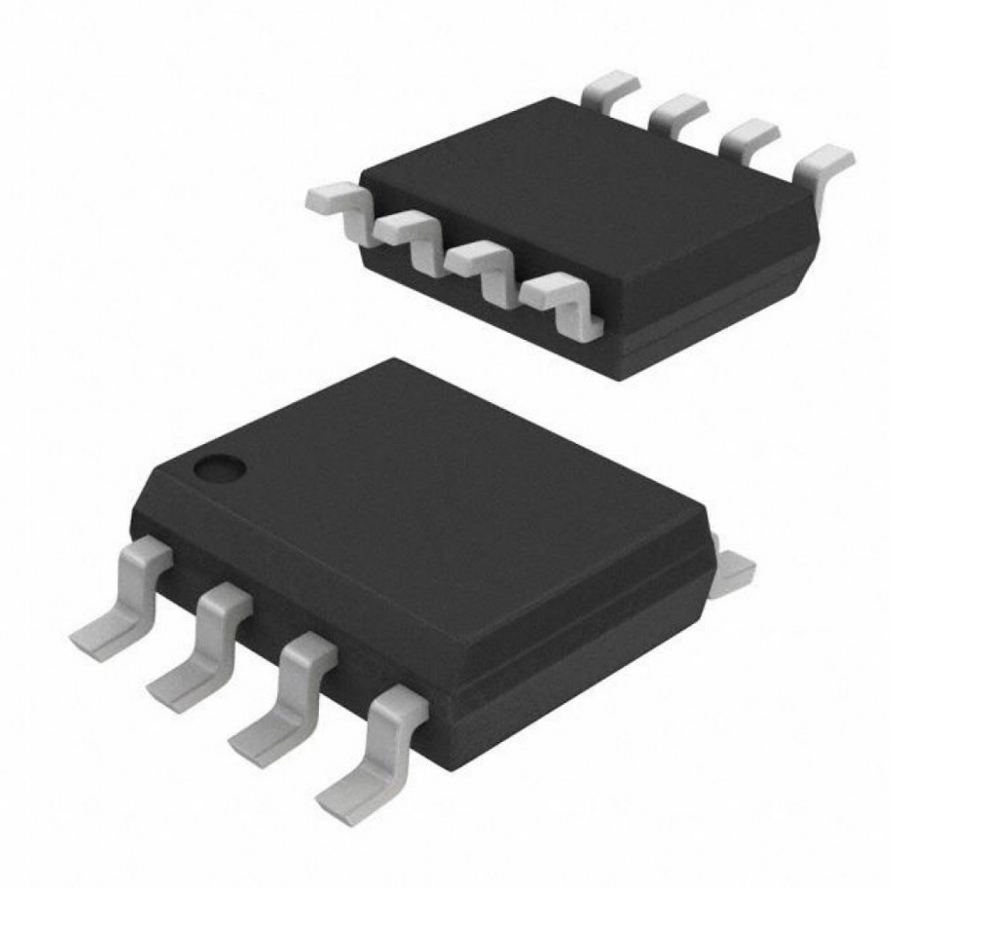
Транзистор полевой AO4614B / N+P-канал, SO-8
У поставщика
ПроизводительA&O
КатегорияТранзисторы
У поставщиков
1 026 шт.
Норм. уп.: 3000
Цены поставщиков
Склад 13
В наличии:1 026 шт
Срок поставки: до недели
Норм. уп.: 3000
Минимальная партия: 20 шт
| Кол-во, шт. | Цена, ₽ |
|---|---|
| от 1 | 36,70 |
| от 62 | 33,41 |
| от 124 | 30,69 |
| от 248 | 28,66 |
| от 496 | 27,13 |
Описание
Транзистор полевой AO4614B производства A&O — это сдвоенный MOSFET-ключ с комплементарной структурой (N+P-канал) в компактном корпусе SO-8. Компонент оптимизирован для низковольтных схем, где требуется коммутация нагрузки с разной полярностью. Благодаря низкому сопротивлению открытого канала и высокой скорости переключения подходит для DC/DC-преобразователей, цепей защиты от переполюсовки и портативной электроники.
Технические характеристики
| Корпус | SOIC-8 |
| Тип монтажа | SMD |
| Описание | 40V Dual P + N-Channel MOSFET |
| Артикул | AO4614B |
| Channel type | N-Channel and P-Channel |
| Gate resistance n | 4.6Ω |
| Gate resistance p | 14Ω |
| Avalanche current n | 14A |
| Avalanche current p | -20A |
| Gate drain charge n | 1.4nC |
| Gate drain charge p | 3.2nC |
| Input capacitance n | 410pF to 650pF |
| Input capacitance p | 750pF to 1175pF |
| Turn on rise time n | 3.6ns |
| Turn on rise time p | 8.4ns |
| Gate source charge n | 2.4nC |
| Gate source charge p | 3.4nC |
| Output capacitance n | 82pF |
| Output capacitance p | 97pF |
| Turn off fall time n | 6.6ns |
| Turn off fall time p | 41.2ns |
| Turn on delay time n | 6.4ns |
| Turn on delay time p | 6.2ns |
| Gate source voltage n | ±20V |
| Gate source voltage p | ±20V |
| Turn off delay time n | 16.2ns |
| Turn off delay time p | 44.8ns |
| Drain source voltage n | 40V |
| Drain source voltage p | -40V |
| Pulsed drain current n | 30A |
| Pulsed drain current p | -30A |
| Diode forward voltage n | 0.76V to 1V |
| Diode forward voltage p | -0.76V to -1V |
| Power dissipation 25c n | 2W |
| Power dissipation 25c p | 2W |
| Power dissipation 70c n | 1.28W |
| Power dissipation 70c p | 1.28W |
| Total gate charge 10v n | 8.9nC to 10.8nC |
| Total gate charge 10v p | 17nC to 22nC |
| Тип упаковки | Tape and Reel (лента в катушке) |
| Gate threshold voltage n | 1.7V to 3V |
| Gate threshold voltage p | -1.7V to -3V |
| On state drain current n | 30A |
| On state drain current p | -30A |
| Total gate charge 4 5v n | 4.3nC to 5.6nC |
| Total gate charge 4 5v p | 7.9nC to 10nC |
| Continuous drain current n | 6A |
| Continuous drain current p | -5A |
| Forward transconductance n | 19S |
| Forward transconductance p | 13S |
| Gate body leakage current n | ±100nA |
| Gate body leakage current p | ±100nA |
| Описание (англ.) | field-effect transistor assembly, N+P-channel, 40V 6/5A |
| Repetitive avalanche energy n | 9.8mJ |
| Repetitive avalanche energy p | 20mJ |
| Continuous drain current n 70c | 5A |
| Continuous drain current p 70c | -4A |
| Reverse transfer capacitance n | 43pF |
| Reverse transfer capacitance p | 72pF |
| Drain source breakdown voltage n | 40V |
| Drain source breakdown voltage p | -40V |
| Zero gate voltage drain current n | 1µA |
| Zero gate voltage drain current p | -1µA |
| Body diode reverse recovery time n | 18ns to 24ns |
| Body diode reverse recovery time p | 21ns to 27ns |
| Junction storage temperature range | -55 to 150°C |
| Body diode reverse recovery charge n | 10nC |
| Body diode reverse recovery charge p | 14nC |
| Zero gate voltage drain current 55c n | 5µA |
| Zero gate voltage drain current 55c p | -5µA |
| Maximum body diode continuous current n | 2A |
| Maximum body diode continuous current p | -2A |
| Static drain source on resistance 10v n | 24mΩ to 30mΩ |
| Static drain source on resistance 10v p | 36mΩ to 45mΩ |
| Static drain source on resistance 4 5v n | 30mΩ to 38mΩ |
| Static drain source on resistance 4 5v p | 50mΩ to 63mΩ |
| Thermal resistance junction ambient 10s n | 62.5°C/W |
| Thermal resistance junction ambient 10s p | 62.5°C/W |
| Thermal resistance junction lead steady n | 50°C/W |
| Thermal resistance junction lead steady p | 50°C/W |
| Static drain source on resistance 10v 125c n | 36mΩ to 45mΩ |
| Static drain source on resistance 10v 125c p | 52mΩ to 65mΩ |
| Thermal resistance junction ambient steady n | 110°C/W |
| Thermal resistance junction ambient steady p | 110°C/W |
Заметили ошибку в описании или параметрах?