
Документация
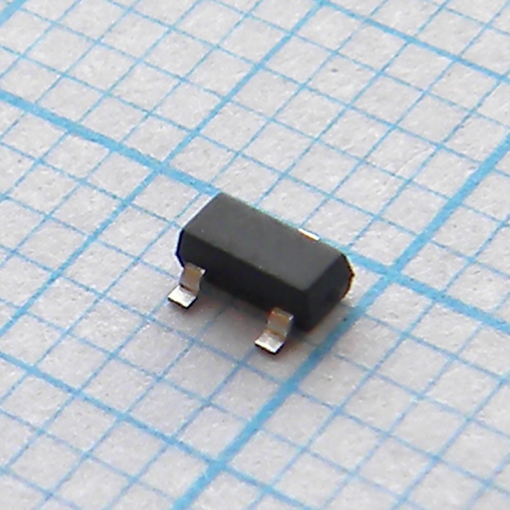
Транзистор полевой MOSFET P-канальный 30В 4А 1,4Вт
У поставщика
ПроизводительA&O
КатегорияТранзисторы полевые (FETs, MOSFETs)
У поставщиков
13 170 шт.
Норм. уп.: 3000
Цены поставщиков
Склад 13
В наличии:13 170 шт
Срок поставки: до недели
Норм. уп.: 3000
Минимальная партия: 62 шт
| Кол-во, шт. | Цена, ₽ |
|---|---|
| от 1 | 11,44 |
| от 271 | 10,19 |
| от 541 | 9,20 |
| от 1 081 | 8,36 |
| от 2 161 | 7,81 |
Описание
Транзистор полевой MOSFET P-канальный от производителя A&O. Работает при напряжении до 30 В, токе до 4 А и мощности 1,4 Вт. Выполнен в компактном корпусе SOT-23. Подходит для коммутации нагрузок в портативных устройствах и схемах управления питанием.
Технические характеристики
| Примечания | Soa curve: Based on junction-to-ambient thermal impedance measured with device mounted on 1in2 FR-4 board with 2oz copper, assuming TJ(MAX)=150°C; Repetitive rating: Pulse width limited by junction temperature TJ=150°C, initial TJ=25°C; Static characteristics: Obtained using <300μs pulses, duty cycle 0.5% max; Power dissipation based on: TJ=150°C, using ≤10s junction-to-ambient thermal resistance; Thermal resistance measurement: RθJA measured with device mounted on 1in2 FR-4 board with 2oz copper, still air, TA=25°C |
| Корпус | SOT-23 |
| Тип монтажа | SMD |
| Top view | D D D G S |
| Технология | advanced trench technology |
| Bottom view | D G S |
| Описание | 30V P-Channel MOSFET |
| Артикул | AO3401A |
| Тепл. хар-ки | Maximum junction to ambient ta 10s: 70°C/W typ, 90°C/W max; Maximum junction to lead steady state: 63°C/W typ, 80°C/W max; Maximum junction to ambient steady state: 100°C/W typ, 125°C/W max |
| Тип упаковки | Tape and Reel (лента в катушке) |
| Предельные значения | Gate source voltage vgs: ±12V; Drain source voltage vds: -30V; Power dissipation ta 25c: 1.4W; Power dissipation ta 70c: 0.9W; Pulsed drain current idm: -27A; Continuous drain current ta 25c: -4A; Continuous drain current ta 70c: -3.2A; Junction and storage temperature range: -55 to 150°C |
| Электрические характеристики | Static parameters: Diode forward voltage vsd: Max: -1V; Typ: -0.7V; Condition: IS=-1A, VGS=0V; Forward transconductance gfs: Typ: 17S; Condition: VDS=-5V, ID=-4.0A; On state drain current id on: Min: -27A; Condition: VGS=-10V, VDS=-5V; Gate threshold voltage vgs th: Max: -1.3V; Min: -0.5V; Typ: -0.9V; Condition: VDS=VGS, ID=-250μA; Gate body leakage current igss: Max: ±100nA; Condition: VDS=0V, VGS=±12V; Drain source breakdown voltage bvdss: Min: -30V; Condition: ID=-250mA, VGS=0V; Zero gate voltage drain current idss: Min: -1μA; At 55c: -5μA; Condition: VDS=-30V, VGS=0V; Maximum body diode continuous current is: -2A; Static drain source on resistance rds on: Vgs 10v id 4a: Max: 50mΩ; Typ: 41mΩ; At 125c: 62mΩ typ, 75mΩ max; Condition: VGS=-10V, ID=-4.0A; Vgs 2 5v id 2 5a: Max: 85mΩ; Typ: 60mΩ; Condition: VGS=-2.5V, ID=-2.5A; Vgs 4 5v id 3 5a: Max: 60mΩ; Typ: 47mΩ; Condition: VGS=-4.5V, ID=-3.5A; Dynamic parameters: Gate resistance rg: Max: 7.8Ω; Min: 12Ω; Typ: 4Ω; Condition: VGS=0V, VDS=0V, f=1MHz; Input capacitance ciss: Typ: 645pF; Condition: VGS=0V, VDS=-15V, f=1MHz; Output capacitance coss: Typ: 80pF; Condition: VGS=0V, VDS=-15V, f=1MHz; Reverse transfer capacitance crss: Typ: 55pF; Condition: VGS=0V, VDS=-15V, f=1MHz; Switching parameters: Turn on rise time tr: Typ: 3.5ns; Condition: VGS=-10V, VDS=-15V, RL=3.75Ω, RGEN=3Ω; Gate drain charge qgd: Typ: 2.5nC; Condition: VGS=-10V, VDS=-15V, ID=-4.0A; Turn off fall time tf: Typ: 9ns; Condition: VGS=-10V, VDS=-15V, RL=3.75Ω, RGEN=3Ω; Gate source charge qgs: Typ: 1.5nC; Condition: VGS=-10V, VDS=-15V, ID=-4.0A; Total gate charge qg 10v: Typ: 14nC; Condition: VGS=-10V, VDS=-15V, ID=-4.0A; Turn on delay time td on: Typ: 6.5ns; Condition: VGS=-10V, VDS=-15V, RL=3.75Ω, RGEN=3Ω; Total gate charge qg 4 5v: Typ: 7nC; Condition: VGS=-4.5V, VDS=-15V, ID=-4.0A; Turn off delay time td off: Typ: 41ns; Condition: VGS=-10V, VDS=-15V, RL=3.75Ω, RGEN=3Ω; Body diode reverse recovery time trr: Typ: 11ns; Condition: IF=-4.0A, dI/dt=100A/μs; Body diode reverse recovery charge qrr: Typ: 3.5nC; Condition: IF=-4.0A, dI/dt=100A/μs |
| Описание (англ.) | Field-effect transistor, P-channel, 30 V, 4 A, 14 W |
Заметили ошибку в описании или параметрах?